My main research interest is investigating the fabrication and operation of semiconductor devices and sensors. Within this broad scope, the three main topics of my research are the application of semiconductor films, such as metal oxides and two-dimensional materials for gas sensing, modeling fabrication processes which are critical for More Moore and More-than-Moore devices, and investigating reliability in back-end-of-line metalization.
Semiconductor Sensors
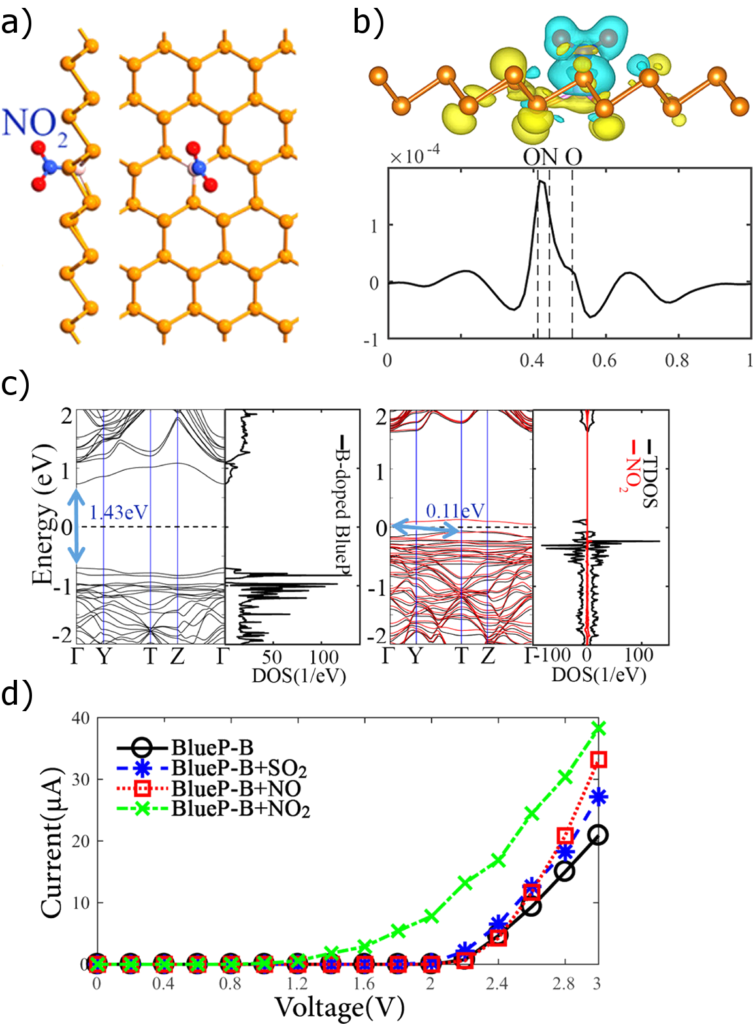
While aggressive transistor scaling has been at the forefront of developments in the semiconductor industry for decades, there is currently an increasing demand for added functionalities in a single device, usually referred to as More-than-Moore integration. This is most evident in the rapid development of integrated smart sensors in many industries, including smart homes, auto, and health, and the rise of wireless sensor networks and the Internet of Things. In my group, we investigate the three-dimensional (3D) integration of gas sensors, including those based on two-dimensional (2D) films, such as graphene, molybdenum disulfide (MoS2), and phosphorene as well as those based on semiconductor metal oxide (SMO) films, such as tin dioxide (SnO2) and zinc oxide (ZnO). For example, we have shown that substitutional doping of blue phosphorene with boron atoms results in an improved selective sensitivity towards NO2, compared to NO and SO2, shown in Fig. 1. 2D semiconductor based gas sensors also have great potential in integration with mature CMOS technology, as they can be introduced during back-end-of-line (BEOL) fabrication. SMO sensors, on the other hand, require heating to elevated temperatures during sensing. For these, we investigate microheater designs and the thermo-electro-mechanical reliability of these complex structures.
Process TCAD
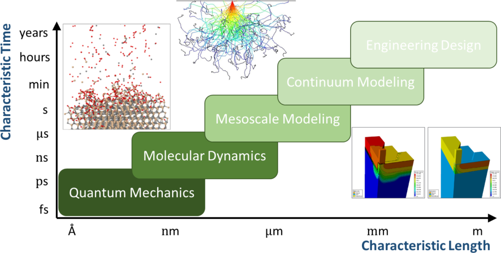
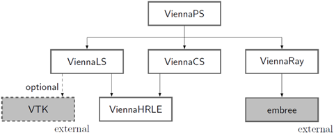
In order to understand how semiconductor devices are fabricated, we often rely on process technology computer aided design (TCAD) simulations. These types of simulations include a variety of models for topography motion during etching and deposition, material modification during ion implantation and annealing, or material growth during oxidation. To fabricate a complete integrated circuit (IC), these additions and modifications occur in several patterning cycles which include photolithography, as given in Fig. 2. Our research encompasses the modeling and simulation of a wide number of relevant processes using advanced simulation frameworks and high performance algorithms. We study processes at all time and size scales, shown in Figure 2. We also build our own simulation tools (Fig. 3), which is offered as Open Access, and which encompasses all levels of extraction, from physical models which use Monte Carlo Ray Tracing to process emulation using Geometric Advection, which was developed in our group.
Interconnect Reliability
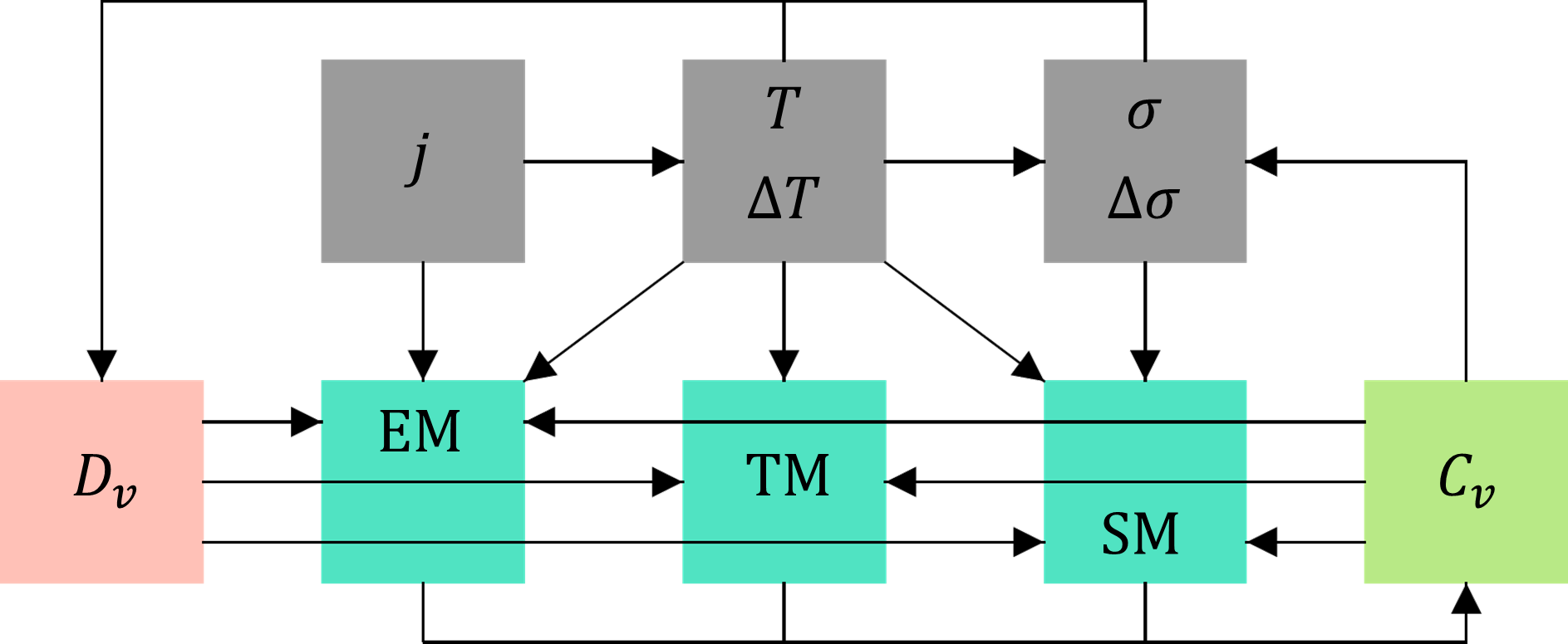
Interconnect is a term given to any conductive layer (most often metal) which is used in integrated circuits (ICs) to electrically contact different devices or chips. The size of these layers can be in the nanometer range, used to contact to the transistors themselves during BEOL fabrication or in the micrometer range, used to stack wafers with different functionalities together through two-and-a-half dimensional (2.5D) or 3D integration. My group works on simulation vacancy and atom dynamics under electro-migration (EM), thermo-migration (TM), and stress-migration (SM), which combines many physical phenomena, including current flow (j), temperature (T), stress (σ), and material diffusivity (Dv) in order to obtain the vacancy concentration Cv, as shown in Fig. 4. We perform these simulations for highly scaled copper wires, where proper treatment of grain boundaries and material interfaces is essential, as well as in microheaters, where thermo-migration plays the main role in vacancy dynamics.